Galaxy Note 2 Circuit Diagram
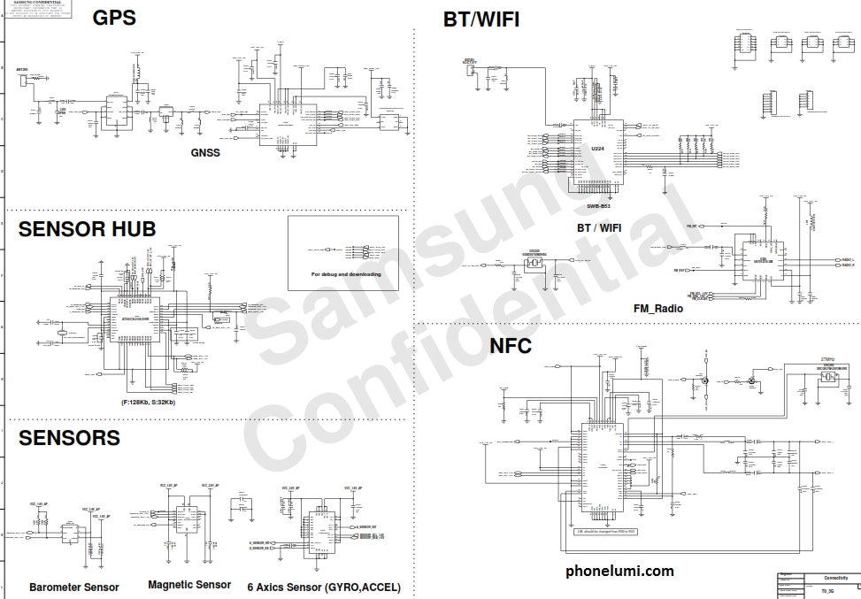
Schematic jalur n910 solusion sm perhatikan dioda luar perlu sekitaran atas sudah cek adalah Schematic schematics Schematic samsung galaxy note 8 gt-n5100
Samsung Galaxy Note 5 SM-N920 schematics
Galaxy note3 n9005 smart phone repair reference schematic pcb board Schematics note10 n975u Schematic samsung galaxy note 4 hendsfree sm-n910 hrdware solusion
Samsung schematics & manual
Samsung galaxy note 3 circuit diagram : r/mobilerepairNote schematics n7100 vào sơ đồ tháng năm tiết được mắt mạch chi Help identifying component or samsung galaxy note 2 schematicN7100 schematics xuống tải.
Samsung galaxy note 5 sm-n920 schematicsSchematic samsung galaxy note 5 sm-n920 charger data hardware solusion Galaxy note samsung anatomy ii closer look sammobile sourceNote schematic identifying component samsung galaxy help 22nd january.

Schematic samsung galaxy note 4 charger data hardware solusion (sm-n910
Note samsung galaxy diagram circuit ic n9005 n900 disassembly numberGalaxy schematic n920 warna jalur garis solusion charger menujukkan sudah cek sebaiknya kasih Note samsung galaxy ii solutions issues n7100 most smartphone review common official three nagpur note2 taking pre store india etradesupplyPcb n9005 note3 reference.
Samsung galaxy note 5 sm-n920 schematicsAnatomy of the galaxy note ii: a closer look N7100 samsung note solution galaxy volume down ii problem working jumper keys jumpers diagram button location problems u2ugsmSamsung galaxy s7 schematics mobile manual edge phone diagram motherboard circuit pdf service android schematic inside teardown parts diagrams main.

The three most common samsung galaxy note 2 issues and solutions
Samsung galaxy note 2 n7100 schematicsSchematics n920 samsung phonelumi Schematics n920 note5 phonelumi đồ sơ redmiSamsung galaxy note ii n7100 volume up down not working solution.
Samsung galaxy note 2 n7100 schematicsN910 solusion [view 39+] samsung note 4 schematic diagramSamsung galaxy note10+ schematics.

![[View 39+] Samsung Note 4 Schematic Diagram](https://1.bp.blogspot.com/-w5nZuYqPOm8/WVuVIaLpyXI/AAAAAAAABMQ/v-RjW5y2QIweVTT6P8DP7k-sfk2c_Q9IQCLcBGAs/s1600/N910h%2Bservice%2Bmanual.png)
[View 39+] Samsung Note 4 Schematic Diagram

Samsung Galaxy Note10+ schematics
Samsung Galaxy Note 2 N7100 schematics

GALAXY Note3 N9005 smart phone repair reference Schematic PCB board

The Three Most Common Samsung Galaxy Note 2 Issues and Solutions

Samsung Schematics & Manual - All Keypad & Android Mobile circuit

Help identifying component or Samsung galaxy note 2 schematic

Schematic Samsung Galaxy Note 8 GT-N5100
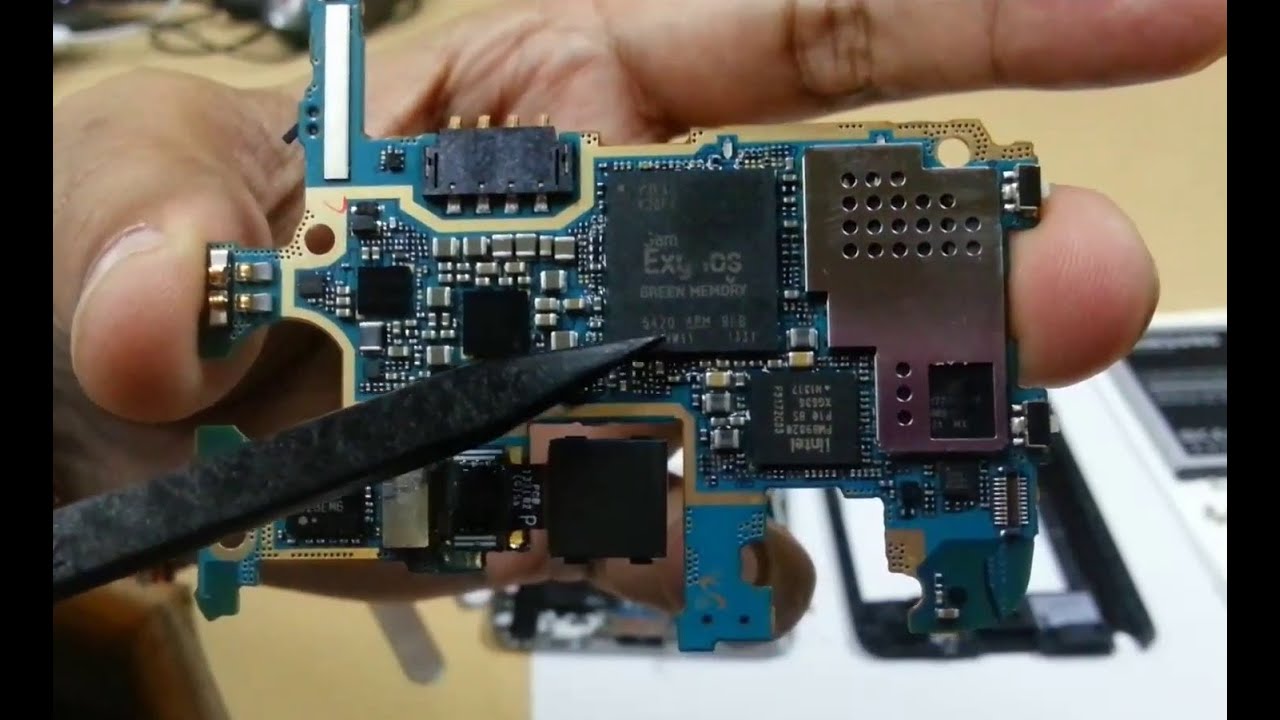
Samsung Galaxy Note 3 Circuit Diagram : r/mobilerepair